
Start Chapter MCQ Quiz
📘 Download Chapter Notes (PDF)
Master Guide: Class 12 Physics Chapter 14 Semiconductor Notes
Introduction: The Solid-State Revolution | Class 12 Physics Chapter 14 Semiconductor Notes
Hello class! Welcome to Chapter 14. Have you ever wondered how computers the size of entire rooms in the 1940s shrank down to the ultra-thin smartphones in our pockets today? The answer lies entirely in this chapter. Let’s dive into the fascinating world of semiconductors!
To control the flow of electrons—the fundamental requirement of any electronic circuit—early scientists relied on vacuum tubes, also known as valves. These included vacuum diodes, triodes, and pentodes. In these bulky devices, electrons were emitted by a heated cathode and traveled through a vacuum to reach an anode. A vacuum was absolutely necessary; otherwise, electrons would collide with air molecules and lose their energy. Furthermore, electrons in these tubes could only flow in one single direction.
But vacuum tubes had major drawbacks: they were huge, required massive amounts of power, operated at high voltages (around 100 V), and had a very limited lifespan. The real breakthrough happened in the 1930s and 1940s with the discovery of solid-state semiconductors. In these modern devices, the charge carriers flow entirely *within* the solid material itself. We don’t need a vacuum, we don’t need external heating, and they operate at incredibly low voltages while lasting almost forever.
1. Classification of Materials: Conductors, Insulators, and Semiconductors
1.1 Based on Conductivity and Resistivity
Before we can understand devices, we must understand the materials. Based on their electrical conductivity ($\sigma$) and resistivity ($\rho$), we can categorize solids into three main groups:
- Metals (Conductors): These materials easily allow current to pass. They have extremely low resistivity ($\rho \sim 10^{-2}$ to $10^{-8} \Omega\text{ m}$) and high conductivity ($\sigma \sim 10^{2}$ to $10^{8} \text{ S m}^{-1}$).
- Insulators: These block the flow of current. They have incredibly high resistivity ($\rho \sim 10^{11}$ to $10^{19} \Omega\text{ m}$) and practically zero conductivity.
- Semiconductors: The heroes of our chapter! Their resistivity and conductivity fall right in the middle, between metals and insulators. Examples include elemental semiconductors like Silicon (Si) and Germanium (Ge), as well as compound semiconductors like GaAs or CdS.
1.2 Based on Energy Bands (The Band Theory)
Teacher’s Note: This is a highly tested concept in CBSE exams. Pay close attention to the energy gaps!
In an isolated atom, electrons orbit in specific, discrete energy levels. However, when billions of atoms come close together to form a solid crystal lattice, their outer orbits overlap and interact. Because no two electrons can have the exact same energy and position, these discrete energy levels split and merge to form continuous ranges of energy called Energy Bands.
- Valence Band (VB): The energy band containing the valence electrons. At absolute zero, it is completely full.
- Conduction Band (CB): The band located just above the valence band. If electrons can reach this band, they become free to move and conduct electricity.
- Energy Gap ($E_g$): Also known as the forbidden gap. This is the energy difference between the lowest level of the conduction band ($E_C$) and the highest level of the valence band ($E_V$). No electrons can exist in this gap.
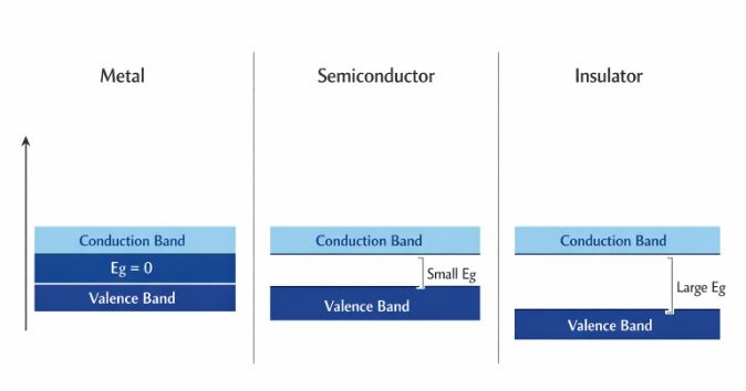
Figure-1: Energy band diagrams illustrating the gap ($E_g$) between the Valence Band and Conduction Band.
How the Band Theory categorizes materials:
- Metals: The conduction band is either partially filled, or the valence and conduction bands completely overlap ($E_g \approx 0$). Electrons can easily slide into the conduction band, giving high conductivity.
- Insulators: There is a massive energy gap ($E_g > 3 \text{ eV}$). Thermal energy at room temperature is nowhere near enough to kick an electron across this giant forbidden gap.
- Semiconductors: There is a small, finite energy gap ($E_g < 3 \text{ eV}$). For Silicon, $E_g = 1.1 \text{ eV}$, and for Germanium, $E_g = 0.7 \text{ eV}$. At absolute zero ($0\text{ K}$), the conduction band is completely empty, making it a perfect insulator. But at room temperature, some electrons gain enough thermal energy to jump the gap into the conduction band, allowing a small amount of conductivity.
2. Intrinsic Semiconductors (The Pure Form)
An intrinsic semiconductor is one that is perfectly pure, without any impurities. Let’s take the most common examples: Silicon (Si) and Germanium (Ge). Both belong to Group 14 of the periodic table, meaning they have 4 valence electrons.
In their crystal lattice, every Si atom forms covalent bonds by sharing its 4 valence electrons with 4 neighboring Si atoms. At low temperatures, all bonds are intact, and there are no free electrons.
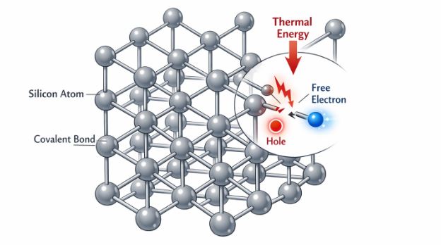
Figure-2: Generation of an electron-hole pair in an intrinsic semiconductor due to thermal energy.
2.1 The Concept of a “Hole”
When the temperature rises, thermal energy vibrates the lattice and breaks a few covalent bonds. The electron that breaks free wanders into the lattice as a conduction electron.
But something equally important happens: when the electron leaves, it leaves behind an empty space or a vacancy in the bond. This vacancy has an effective positive charge because it is missing an electron. We call this vacancy a hole.
If a neighboring bound electron jumps over to fill this hole, it leaves a new hole at its original position. Therefore, the hole appears to move through the crystal just like a positively charged particle!
Mathematical Condition: In an intrinsic semiconductor, every time an electron jumps to the conduction band, it creates exactly one hole in the valence band. Therefore, the number density of electrons ($n_e$) is strictly equal to the number density of holes ($n_h$).
$$n_e = n_h = n_i$$
Where $n_i$ is the intrinsic carrier concentration.
The total current $I$ inside the semiconductor is the sum of the electron current ($I_e$) and the hole current ($I_h$):
$$I = I_e + I_h$$
3. Extrinsic Semiconductors (The Doped Form)
Here is a practical problem: at room temperature, pure Silicon’s conductivity is simply too low to be useful for making devices like phone processors. To fix this, we deliberately add specific, desirable impurities to the pure crystal. This process is called doping, and the resulting material is an extrinsic semiconductor.
The impurity (dopant) must be carefully chosen so that it roughly matches the size of the Si/Ge atoms and doesn’t distort the crystal lattice. We add just a tiny amount—typically a few parts per million (ppm).
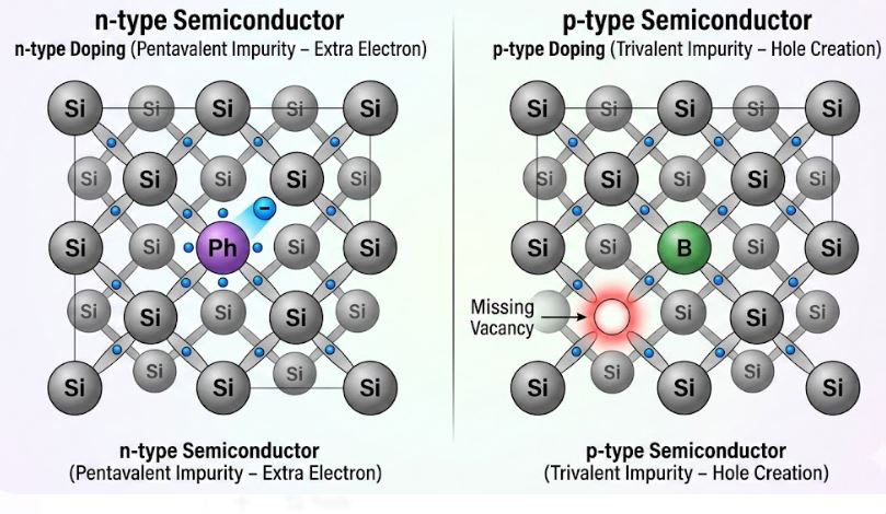
Figure-3: (Left) n-type doping with a pentavalent atom donating a free electron. (Right) p-type doping with a trivalent atom creating a hole.
3.1 n-type Semiconductor
We create an n-type semiconductor by doping Silicon with a pentavalent impurity (an element from Group 15 with 5 valence electrons), such as Arsenic (As), Antimony (Sb), or Phosphorus (P).
- When a pentavalent atom takes the place of a Si atom, it uses 4 of its electrons to form covalent bonds with 4 neighboring Si atoms.
- The 5th electron has no atom to bond with. It remains very weakly bound to the parent impurity atom.
- It takes very little energy ($\sim 0.05 \text{ eV}$ for Si) to set this 5th electron completely free into the conduction band. Thus, the pentavalent atom is called a donor impurity.
- Carrier Concentration: Because every donor atom gives one free electron, electrons vastly outnumber holes. Electrons are the majority carriers, and holes are the minority carriers.
$$n_e \gg n_h$$
3.2 p-type Semiconductor
We create a p-type semiconductor by doping Silicon with a trivalent impurity (an element from Group 13 with 3 valence electrons), such as Boron (B), Aluminum (Al), or Indium (In).
- The trivalent atom can only form 3 covalent bonds with its neighbors. The 4th bond is incomplete, resulting in a vacancy or a hole.
- A neighboring bound electron can easily jump into this hole, effectively making the trivalent atom negatively charged while the hole moves freely through the lattice. The trivalent atom is called an acceptor impurity.
- Carrier Concentration: Every acceptor atom creates a hole. Therefore, holes are the majority carriers, and electrons are the minority carriers.
$$n_h \gg n_e$$
Teacher’s Pro-Tip: A very common exam trick is asking about the net electrical charge of an n-type or p-type semiconductor. Remember: They are electrically NEUTRAL! Although we have extra electrons or holes acting as charge carriers, the total number of protons in the nuclei still perfectly balances the total number of electrons in the entire crystal.
The Mass Action Law: In thermal equilibrium, for any extrinsic semiconductor, the product of electron and hole concentrations remains constant:
$$n_e n_h = n_i^2$$
4. The p-n Junction: The Heart of Electronics
You cannot just take a block of p-type silicon, press it against a block of n-type silicon, and expect it to work!. The surface roughness would be too great. Instead, a p-n junction must be manufactured seamlessly by doping one side of a continuous Silicon wafer with acceptors and the other side with donors.
When this metallurgical junction forms, two vital processes immediately take place: Diffusion and Drift.
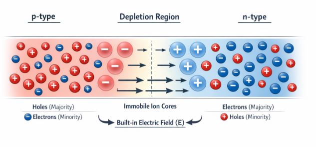
Figure-4: Formation of the depletion region in a p-n junction and the resulting built-in electric field.
- Diffusion: On the n-side, there is a huge concentration of electrons. On the p-side, there is a huge concentration of holes. Naturally, electrons want to diffuse from the n-side to the p-side, and holes diffuse from the p-side to the n-side. This causes a diffusion current.
- Formation of the Depletion Region: When an electron leaves the n-side, it leaves behind an uncompensated, positively charged donor ion. Because it is an ion locked in the crystal lattice, it is immobile. Similarly, when a hole diffuses from the p-side, it leaves behind a negatively charged immobile acceptor ion. This creates a space near the junction entirely depleted of free mobile charge carriers. We call this the Depletion Region.
- Barrier Potential and Drift: The positive ions on the n-side and negative ions on the p-side act like a tiny built-in battery, creating an electric field pointing from n to p. This electric field acts as a barrier, stopping any more majority carriers from diffusing across. This built-in voltage is called the Barrier Potential ($V_0$). However, this same electric field takes any minority carriers that wander near the junction and sweeps them across to the other side. This motion due to the electric field is called drift current.
At equilibrium, the junction is stable because the Diffusion Current is exactly equal and opposite to the Drift Current, making the net current zero.
5. The Semiconductor Diode and Biasing
A semiconductor diode is simply a p-n junction equipped with metallic contacts at the ends so we can connect it to an external battery. It is a two-terminal device. The magical property of a diode is that it allows current to flow easily in one direction, but strongly blocks it in the other. We control this by “biasing” the diode with an external voltage ($V$).
5.1 Forward Bias
A diode is forward-biased when the p-side is connected to the positive terminal of the battery and the n-side to the negative terminal.
- The external voltage directly opposes the built-in barrier potential ($V_0$).
- As a result, the effective barrier height is reduced to ($V_0 – V$).
- The depletion region width decreases.
- Majority carriers are pushed across the junction. Electrons cross over to the p-side (where they become minority carriers), and holes cross to the n-side. This is called minority carrier injection.
- The result is a large forward current, typically measured in milliamperes (mA), dominated by diffusion.
5.2 Reverse Bias
A diode is reverse-biased when the n-side is connected to the positive terminal and the p-side to the negative terminal.
- The external voltage now aligns with the built-in barrier potential.
- The effective barrier height increases to ($V_0 + V$).
- The depletion region widens significantly.
- Majority carriers are pulled away from the junction. The diffusion current practically drops to zero.
- However, the strong electric field sweeps the thermally generated minority carriers across the junction. This creates a very small, constant current called the reverse saturation current, measured in microamperes ($\mu\text{A}$).
- If the reverse voltage gets too high, the diode hits its breakdown voltage ($V_{br}$), causing a massive surge in current which will destroy a normal diode due to overheating.
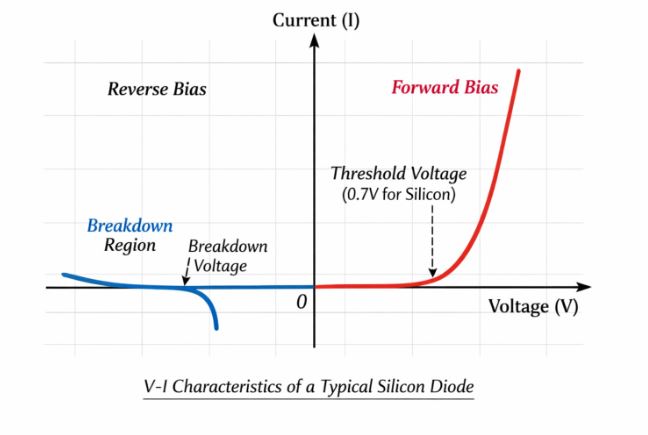
Figure-5: V-I characteristics of a typical Silicon diode. Note the threshold voltage in forward bias and the breakdown in reverse bias.
Dynamic Resistance: Because the V-I graph is not a straight line (it does not obey Ohm’s Law linearly), we define dynamic resistance ($r_d$) at a specific operating point as the ratio of a small change in voltage to the resulting small change in current:
$$r_d = \frac{\Delta V}{\Delta I}$$
6. Application of Junction Diode as a Rectifier
The electricity coming into our homes is Alternating Current (AC), which constantly reverses direction. But your laptop and mobile phone need Direct Current (DC) to charge. Since a diode only allows current to pass when it is forward-biased, it is the perfect tool to convert AC into DC. This process is called Rectification, and the circuit is a Rectifier.
6.1 Half-Wave Rectifier
A half-wave rectifier uses a single diode connected in series with a load resistor ($R_L$). An AC voltage is supplied via a transformer.
- During the positive half-cycle of the AC input, the diode is forward-biased and conducts current. A voltage appears across the load.
- During the negative half-cycle, the diode is reverse-biased. It blocks the current, and no voltage appears across the load.
- Result: We only get output for half the time. The output is a series of positive pulses. It is unidirectional but still pulsating.
6.2 Full-Wave Rectifier
To be more efficient, we use a Full-Wave Rectifier, which requires a centre-tap transformer and two diodes ($D_1$ and $D_2$).
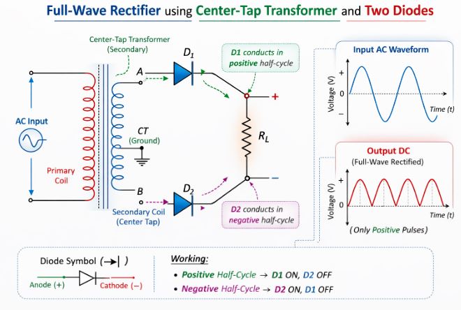
Figure-6: The Full-Wave Rectifier circuit. $D_1$ conducts during one half-cycle, and $D_2$ conducts during the other, ensuring continuous output.
- The ends of the transformer secondary are connected to the p-sides of the diodes, and their n-sides are tied together. The load is connected between this common point and the centre-tap (ground).
- During the first positive half-cycle, point A is positive and point B is negative. Diode $D_1$ is forward-biased and conducts, while $D_2$ is reverse-biased and blocks. Current flows through the load.
- During the next half-cycle, the polarities flip. Point B is positive and point A is negative. Now, diode $D_2$ is forward-biased and conducts, while $D_1$ is blocked. Because of the circuit layout, the current still flows through the load in the exact same direction.
- Result: We get a continuous, unidirectional output. It is much more efficient than the half-wave rectifier.
6.3 Filter Circuits
The output from a full-wave rectifier is unidirectional, but it is still bumpy or “pulsating”. Devices need steady, flat DC voltage. To smooth out these ripples, we connect a large Capacitor in parallel with the load resistor.
When the voltage pulse rises, the capacitor charges up to the peak voltage. When the voltage from the rectifier begins to fall, the capacitor discharges stored energy through the load, keeping the output voltage high until the next pulse arrives to recharge it. This results in a nearly pure, steady DC voltage.
Common Student Misconceptions (Avoid These!)
- Misconception: “A p-type semiconductor is positively charged.”
Reality: Both p-type and n-type semiconductors are 100% electrically neutral. The terms “p” and “n” refer solely to the majority charge carriers (holes and electrons), but the total atoms themselves are neutral before and after forming the crystal. - Misconception: “Holes are actual physical particles like protons.”
Reality: Holes are simply empty vacancies in covalent bonds where an electron should be. We treat them as positively charged particles only to make the math and physics easier to understand. - Misconception: “The depletion region is full of charges.”
Reality: It is depleted of mobile charge carriers (free electrons and holes). It only contains fixed, immobile ion cores.
Board Exam Practice Set (with Solutions)
Here are some high-yield questions aligned with the CBSE pattern to test your conceptual understanding.
Very Short Answer Questions (1-2 Marks)
Q1. At absolute zero temperature, what is the conductivity of an intrinsic semiconductor? Why?
Answer: At absolute zero ($0\text{ K}$), the conductivity is zero. An intrinsic semiconductor behaves as a perfect insulator because all electrons are bound in covalent bonds in the valence band, and there is no thermal energy to excite them across the energy gap into the conduction band.
Q2. Name the dopants used to make (i) n-type and (ii) p-type semiconductors.
Answer: (i) Pentavalent impurities (valency 5) like Arsenic, Antimony, or Phosphorus for n-type. (ii) Trivalent impurities (valency 3) like Indium, Boron, or Aluminum for p-type.
Short Answer Questions (3 Marks)
Q3. Explain how the depletion region and barrier potential are formed in a p-n junction.
Answer: When a p-n junction is formed, electrons from the n-side diffuse to the p-side due to a concentration gradient, leaving behind immobile positive donor ions. Simultaneously, holes from the p-side diffuse to the n-side, leaving immobile negative acceptor ions. This forms a space-charge region on both sides devoid of free carriers, known as the depletion region. The accumulation of these positive and negative ions sets up an electric field from the n-side to the p-side. This field creates a potential difference called the barrier potential ($V_0$), which opposes further diffusion of majority carriers.
Q4. Draw the V-I characteristics of a p-n junction diode. Why is the current in reverse bias almost independent of the applied voltage up to the breakdown point?
Answer: (Draw Figure 5 showing forward and reverse characteristics). Under reverse bias, the majority carriers are pulled away from the junction, stopping diffusion current. The extremely small reverse current ($\mu\text{A}$) is a drift current caused purely by minority carriers being swept across the junction by the electric field. Because the number of minority carriers depends on temperature and not on the applied voltage, this reverse saturation current remains almost constant until the breakdown voltage is reached.
Long Answer Questions (5 Marks)
Q5. With the help of a circuit diagram, explain the working of a full-wave rectifier. Include input and output waveforms. What is the role of a capacitor filter?
Answer:
A full-wave rectifier converts the complete AC cycle into unidirectional DC. (Draw Figure 6 showing the centre-tap transformer and two diodes).
Working: It utilizes a centre-tap transformer and two diodes, $D_1$ and $D_2$. During the positive half-cycle of the AC input, one end of the secondary (A) is positive, making $D_1$ forward-biased so it conducts, while $D_2$ is reverse-biased and blocks. The current flows through the load resistor $R_L$. During the negative half-cycle, the other end (B) becomes positive, making $D_2$ forward-biased and $D_1$ reverse-biased. Current again flows through $R_L$ in the exact same direction. Thus, we obtain output for both halves of the cycle.
Role of Capacitor: The output of the rectifier is pulsating. A large capacitor is connected in parallel to the load. It charges to the peak voltage and then discharges slowly through the load when the rectifier voltage drops, smoothing out the ripples and providing a steady DC output.
Case-Based Question (4 Marks)
Q6. Read the passage and answer the questions.
Suppose a pure Silicon crystal has $5 \times 10^{28} \text{ atoms m}^{-3}$. It is doped by 1 ppm (parts per million) concentration of pentavalent Arsenic. The intrinsic carrier concentration is $n_i = 1.5 \times 10^{16} \text{ m}^{-3}$.
(i) Which type of semiconductor is formed? (1M)
Answer: Since it is doped with a pentavalent impurity (Arsenic), an n-type semiconductor is formed.
(ii) Calculate the number density of electrons ($n_e$). (1.5M)
Answer: Doping concentration = 1 ppm = 1 atom out of $10^6$ atoms.
Number of dopant atoms $N_D = (5 \times 10^{28}) / 10^6 = 5 \times 10^{22} \text{ m}^{-3}$.
Since the thermally generated electrons are negligibly small compared to those from doping, $n_e \approx N_D = 5 \times 10^{22} \text{ m}^{-3}$.
(iii) Calculate the number density of holes ($n_h$). (1.5M)
Answer: Using the mass action law, $n_e n_h = n_i^2$.
$n_h = (n_i^2) / n_e = (1.5 \times 10^{16})^2 / (5 \times 10^{22})$.
$n_h = (2.25 \times 10^{32}) / (5 \times 10^{22}) \approx 4.5 \times 10^9 \text{ m}^{-3}$.
Assertion-Reasoning Question (1 Mark)
Q7.
Assertion (A): When a p-n junction is forward-biased, the barrier potential decreases.
Reason (R): Under forward bias, the applied external voltage opposes the built-in barrier potential.
Options:
(a) Both A and R are true and R is the correct explanation of A.
(b) Both A and R are true but R is NOT the correct explanation of A.
(c) A is true but R is false.
(d) A is false but R is true.
Answer: (a). The external voltage ($V$) directly drops across the depletion region opposing the built-in potential ($V_0$), reducing the effective barrier height to ($V_0 – V$).
End of Chapter 14 Notes.
Students, mastering semiconductors requires understanding the *why* behind electron and hole movements. Practice sketching the energy band diagrams and the full-wave rectifier circuit, as these appear frequently in exams!
Read Also:
Class-12 Chapter 13 – Nuclei
For official syllabus and textbooks, visit the
NCERT Official Website.